

Product Overview
Five-Output 3.3 V PLL Zero Delay Buffer, 150-mil SOIC, Commercial Grade
Condition
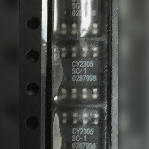
Unused new old stock (NOS). Markings legible: CY2305 SC-1. Sold each.
Same or next business day shipping from our Idaho warehouse. Reliable parts since 1999. Honest pricing, no nonsense.
Satisfaction guaranteed, every time.
Product Overview
Cypress Semiconductor's CY2305SC-1 takes one reference clock and drives five low-skew copies of it, with an on-chip PLL that holds input-to-output delay at zero. It sits in an 8-pin 150-mil SOIC in the standard -1 drive grade.
Key Features
- PLL-based zero delay buffer: one reference input, five clock outputs
- Zero input-to-output propagation delay
- Output-to-output skew 250 ps max, 85 ps typical, with all outputs equally loaded
- Device-to-device skew 700 ps max
- 3.3 V supply, 3.0 V to 3.6 V operating range
- 8-pin 150-mil SOIC, commercial temperature range 0 degC to +70 degC
Applications
- Fanning one board clock out to several loads without adding delay to the copies
- Replacing a failed clock buffer on a 3.3 V board that was built around the CY2305SC-1
Frequently Asked Questions
What does the -1 at the end mean?
It is the standard-drive grade. The -1H versions carry higher output drive; this one is the -1.
Does the buffer add delay between the reference and the outputs?
No. The PLL lines the outputs up with the reference, so input-to-output delay is zero, and the five outputs stay within 250 ps of each other when equally loaded.
Will it run from a 5 V supply?
No. It is a 3.3 V part with a 3.0 V to 3.6 V operating range.
One reference clock walks in and five leave together, the PLL quietly erasing the trip through the chip. If a 3.3 V board is waiting on its clock tree, this little SOIC is ready to hand out the beat.