

Product Overview
Single-Sided Stripboard Prototyping PCB 79x145mm Thai Para UPC 875
Condition
New. Unused prototyping circuit board in clean physical condition with bare copper traces and clear silkscreen grid markings. Sold individually.
Same or next business day shipping from our Idaho warehouse. Reliable parts since 1999. Honest pricing, no nonsense.
Here for our customers, with a satisfaction guarantee that means what it says.
Product Overview
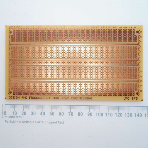
Thai Para Engineering model UPC 875 (distributor SKU A-5462) is an expansive 79 mm by 145 mm single-sided prototyping board built on rigid phenolic paper laminate. Engineered for point-to-point wiring and quick circuit assembly, the board layout features 54 numbered columns and 13 lettered rows (A through M). Continuous horizontal copper rails run along the outer margins and center spans to serve as dedicated power and ground distribution buses, while segmented copper trace groupings accommodate dual in-line IC footprints, passives, and wire-wrap headers at standard 2.54 mm (0.100 in) hole spacing.
Key Features
- 79 mm x 145 mm (approx. 3.11 in x 5.71 in) large-format layout provides ample real estate for complex multi-stage circuits.
- Standard 2.54 mm (0.100 in) hole pitch accepts standard through-hole DIP ICs, sockets, and discrete components.
- 1.00 mm hole diameter accommodates typical component leads and solid interconnect wire.
- 54 columns and 13 rows with coordinate markings etched in copper on solder side and silkscreened on component side.
- Continuous long-axis bus rails simplify power, ground, and signal bus routing across the entire board span.
- Single-sided bare copper traces on phenolic paper laminate for straightforward soldering and trace cutting.
Applications
- Building dedicated analog synth modules, guitar effect circuits, and audio preamps that require spacious component spacing.
- Hardwiring microcontrollers, sensor breakout modules, and peripheral relays into permanent bench fixtures.
- Educational electronics instruction and lab experiments where through-hole circuits must be easily assembled and probed.
- Fabricating one-off industrial test jigs or interface boards without waiting for custom PCB manufacturing turns.
Frequently Asked Questions
What is the grid spacing and lead hole diameter?
The holes are drilled on industry-standard 2.54 mm (0.100 in) centers with a nominal hole diameter of 1.00 mm, fitting standard DIP IC sockets, terminal blocks, headers, and passive components.
How are the copper traces organized on the solder side?
The copper side features horizontal continuous bus traces running along the top, center, and bottom spans for power rail routing, alongside segmented multi-hole strips arranged to bridge DIP IC packages and adjacent components.
Can individual traces be severed to customize the layout?
Yes. Because the board uses single-sided copper on a phenolic substrate, copper runs can be separated using a standard trace cutter, hobby knife, or small drill bit to isolate circuit nodes.
Why buy this individual prototyping board rather than chasing bulk surplus lots?
You get the exact large-format 79x145mm board shown, inspected and ready to solder on your bench, without having to buy an oversized surplus assortment full of odd shapes you will never use. Orders ship flat rate for $8, or free once your order reaches $28, leaving our Idaho warehouse the same or next business day.
Nothing beats the quiet satisfaction of dropping real components onto bare copper and watching a sketch turn into a working circuit. Lay your traces, heat the iron, and bring your build to life.
Need more than one? More pieces cost less each - the price-break table on this page shows what each quantity costs.