
Product Overview
2 Gbit Parallel NAND Flash Memory, 256M x 8, 2.7 to 3.6 V, 48-Pin TSOP I
Condition
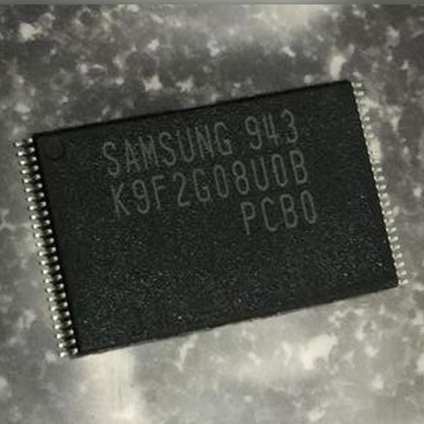
Condition: unused new old stock (NOS). Sold each. Markings legible: SAMSUNG / K9F2G08U0B / PCB0.
Ships same or next business day from our Idaho warehouse. Honest pricing, no nonsense.
Online since 1999. A no-hassle satisfaction guarantee on every order.
Product Overview
A 2 Gbit parallel NAND flash from Samsung, the K9F2G08U0B-PCB0 is organized 256M x 8 with an x8 I/O bus and the CE, RE, WE, ALE, CLE and R/B control lines. It stores data in 2K-byte pages grouped into 128K-byte erase blocks, in a 48-pin TSOP I body.
Key Features
- Density: 2 Gbit (256 MB), 256M x 8; array (256M + 8M) x 8 bit including spare area
- Supply: 2.70 V to 3.60 V
- Page size: (2K + 64) bytes; block size: (128K + 4K) bytes
- Page program 200 us typical; block erase 1.5 ms typical
- Endurance: 100K program/erase cycles with 1 bit per 512 byte ECC
- Data retention: 10 years
- Package: 48-pin TSOP I, 12 x 20 mm, 0.5 mm lead pitch
Applications
- Replacing a failed storage NAND on a router, set-top box or embedded board whose parts list calls for K9F2G08U0B-PCB0
- Loading a saved image in a TSOP48 socket on a universal programmer, then soldering the programmed chip onto the board
- Adding raw x8 NAND storage to a microcontroller or FPGA project with a parallel NAND controller
Frequently Asked Questions
What supply voltage does this chip run on?
2.70 V to 3.60 V. It is the 3.3 V version of the K9F2G08 line.
How much usable storage is 2 Gbit?
256 MB of main array, plus 8 MB of spare area set aside for ECC and bad-block data.
How is this different from the K9F2G08B0B?
The K9F2G08U0B runs from 2.70 V to 3.60 V; the U marks the 3.3 V device. The K9F2G08B0B is the 2.5 V to 2.9 V sibling and does not belong on a 3.3 V rail.
Samsung split the ordering code across the body, K9F2G08U0B on one line and PCB0 beneath it, with 2 Gbit of pages waiting behind 48 fine leads. Load the image in the socket, then solder it down.