

Product Overview
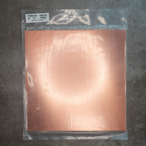
Single-Sided Copper Clad Laminate Sheet for PCB Etching 150 x 150 mm
Condition
Unused new old stock (NOS). Physical condition is clean with intact copper surface and reverse phenolic laminate. Sourced from distributor surplus inventory.
Same or next business day shipping from our Idaho warehouse. Reliable parts since 1999. Honest pricing, no nonsense.
We are here for our customers, with a no-hassle satisfaction guarantee.
Product Overview
PartsMine part number 169287 is a single-sided copper-clad board designed for printed circuit board fabrication, prototyping, and educational electronics projects. Measuring 150 mm by 150 mm (nominal 6 by 6 inches) with a 1.6 mm thickness, this sheet features a uniform 1 oz per square foot copper layer bonded to a sturdy phenolic paper laminate substrate. The reverse side features a repeating printed EC stamp pattern. Suitable for chemical etching, CNC isolation milling, or manual trace scoring.
Key Features
- Single-sided copper cladding with 1 oz/sq ft (35 µm) copper weight
- Phenolic paper laminate substrate providing rigid structural support
- Nominal sheet dimensions of 150 mm x 150 mm (6" x 6")
- Standard 1.6 mm (1/16") overall board thickness
- Reverse face stamped with repeating EC manufacturer identifier
- Manufactured in Taiwan
Applications
- Etching custom single-sided circuit boards using ferric chloride or persulfate solutions
- Isolating circuit traces on a desktop CNC router or PCB milling machine
- Building dead-bug or Manhattan-style RF prototyping modules on a continuous ground plane
- Cutting into custom shapes for small hobby circuits, guitar pedal layouts, and sensor breakouts
Frequently Asked Questions
Can this board be cut to smaller sizes?
Yes. Phenolic paper laminate boards can be sheared, cut with a fine-tooth hobby saw, or scored and snapped along a straight edge.
What method is recommended for applying trace layouts?
This copper surface accepts toner-transfer paper, direct ink resist pen drawing, or photoresist films for ultraviolet exposure.
Why buy this individual board instead of a bulk surplus lot?
Purchasing an individually verified piece ensures you receive clean, flat material ready for immediate bench work without committing to an oversized assortment or sorting through damaged remnants. Shipping is $8 flat rate, free once the order passes $28, and orders leave the Idaho warehouse the same or next business day.
Nothing quite matches the satisfaction of pulling a freshly etched board from the bath and seeing your traces sharp, clean, and ready for solder. Lay down your design, etch your circuit, and bring the prototype to life.